


HTT
The privately held htt group was founded in 1988 in Munich. Under the mission statement “Reliability and a unique value for customers and Suppliers “, the focus of the htt group is to be a major supplier to the Semiconductor Industry by representing well-known leading manufacturers of systems and consumables, tools for Wafer Fab, Wafer […]
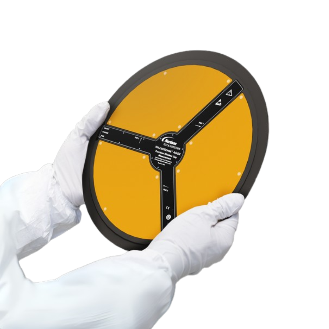
Nordson CyberOptics
Speed your semiconductor processes with WaferSense and ReticleSense measurement devices. When you need the most efficient and effective measurement devices for semiconductor tool set-up and maintenance processes, count on CyberOptics, the global market leader in wireless semiconductor measurement devices for chamber gapping, leveling, wafer handoff teaching, vibration, airborne particle, relative humidity and resistance measurement. Save […]
ePAK
ePAK is a Leading Full-Service Provider of Semiconductor Transfer and Handling Products. Device protection and contamination control begins at the wafer fab and extends to the assembly site. ePAK never forgets that the most valuable product in the semiconductor and electronics industry is also the most fragile and susceptible to mishandling and contamination. Not all […]
Gnone Pad
Advanced Wafer Handling Solutions with GNONE ESD-Pads Technology As materials evolve—like Sapphire, Graphite, Silicon Carbide and more, handling them becomes more complex. Electrostatic charge, slippage, and surface damage are critical risks. Introducing our advanced wafer handling technology for semiconductor equipment – GNONE ESD-Pads Our ESD-Pads technology offers precise handling, controlled electrostatic discharge and excellent anti-slip […]