As materials evolve—like Sapphire, Graphite, Silicon Carbide and more, handling them becomes more complex. Electrostatic charge, slippage, and surface damage are critical risks.
Introducing our advanced wafer handling technology for semiconductor equipment – GNONE ESD-Pads
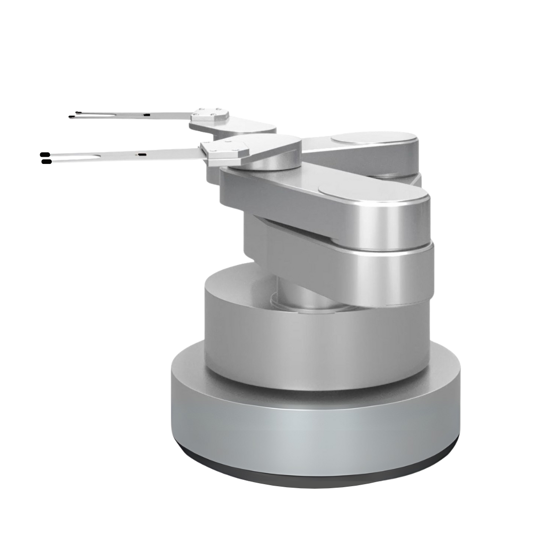
Our ESD-Pads technology offers precise handling, controlled electrostatic discharge and excellent anti-slip gripping, safe and stable wafer transport in high-precision.
– GNONE ESD-safe key points
– Controlled resistivity 10*6 – 10*9 Ohms
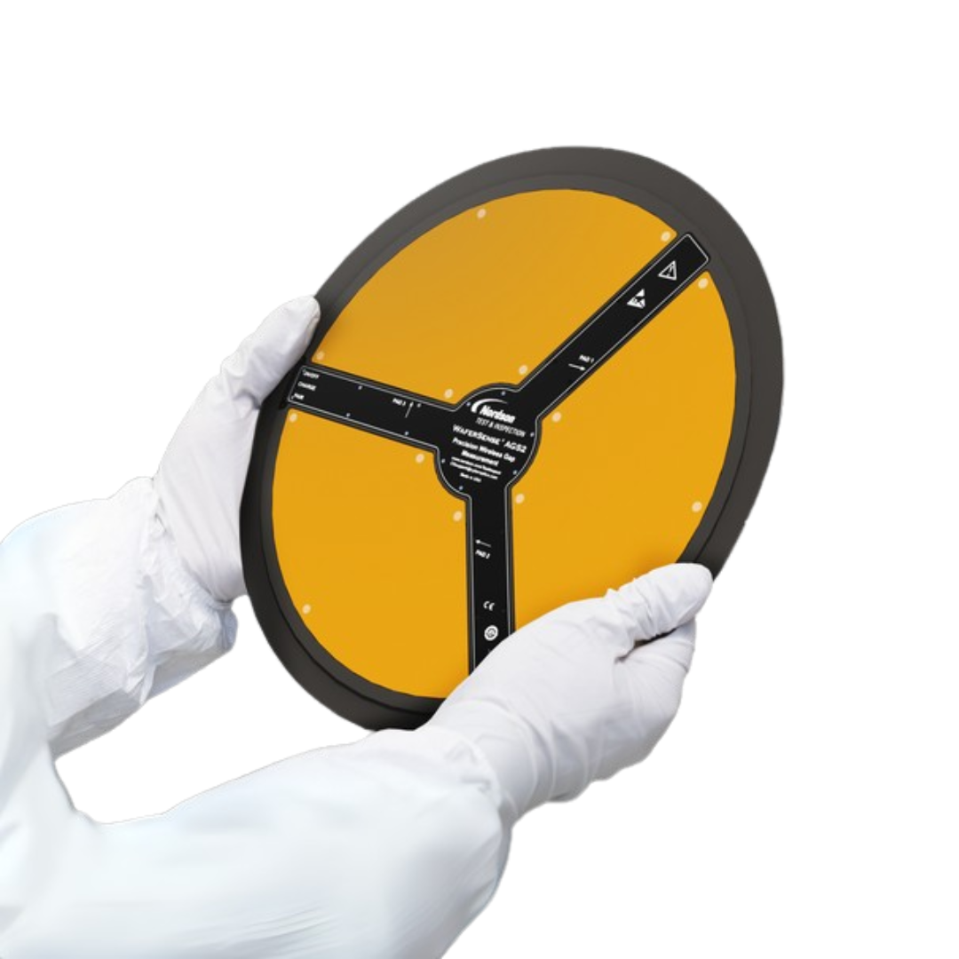
– Applicable for 4″, 6″, 8″, and 12″ wafers and large flat panels
– High grip, Adaptable per each type of application – no wafer slippage
– Handling fragile and hard materials
– Compatible with hi temp warmed environment (tested up to 270°C).
– Boost Robot speed by 2-6 times, maximizing throughput and minimizing wafer breakage.
– Perfect for wrapped wafers up to 8mm thick and various handling applications.
Upgrade your wafer handling with confidence.
Contact us today for a customized solution.